Electronic load using ESP8266
Intro
Long time, no see. Well, let me tell you a thing, parenting is the end of your free time to do your stupid projects. It took me a few months just to complete a very small stupid project like this… Anyway, this time I wanted to build an electronic load. There are so many designs out there with various different user interfaces, but I wanted something more useless than a pot to control the output current. Therefore, I though why not build an electronic load with a web interface? And which is the best option for that? Of course, esp8266. Well… not really, but we’ll see why later. Still, this is build on the esp8266 anyways.
Electronic load circuit
There are various ways to make an eload, but the easiest way to use a N-MOSFET and an opamp that it’s negative feedback drives the Gate-Source of the MOSFET. This is a screenshot of the main circuit:

You can find the kicad project for the eload circuit here:
https://github.com/dimtass/esp8266-web-eload/tree/master/kicad/eload
In the above circuit there’s a first stage opamp that is driven from a DAC. This opamp amplifies the signal with a gain of 2.2 and then the second stage opamp drives the MOSFET. The source of the MOSFET is connected on the PSU under test and the source to an array of parallel 10Ω/1W resistors, which makes an effective 1Ω/10W resistor. The gate and source of the MOSFET are connected in the negative feedback loop of the opamp. This means the opamp will do what opamps do and will mirror the voltage on the (+) input to the (-) input. Which means that whatever voltage is applied on the (+) input then the opamp will drive the output in a way that both inputs have the same voltage. Because the gate and the source of the MOSFET are part of the feedback loop, then in this circuit it means the voltage on the source will be the same as the (+) input. Therefore, if you connect a load that is 1Ω then the current will be I=V/R and because R=1Ω, that means Ι=V. So, if 5V are applied in the (+) input then 5A will flow on the resistors.
It’s generally better to have resistors in parallel, because that means that the current will be split to these resistors, which means less heat and no need for extra cooling on a single resistor.
There is also another opamp which buffers the voltage on the negative loop and drives a voltage divider and an RC filter. We need a buffer there in order not to apply any load on the feedback, as the opamp will draw only a tiny current which doesn’t affect the performance of the circuit. The voltage divider is an 1/10 divider that limits the maximum 10V input to the max 1V allowed ADC input of the esp8266. Then there is a first grade RC filter with a pole at ~1Hz to filter out any noise, as we only care about the DC offset.
As the opamp is powered with a +10V then it means that if it’s a rail-to-rail opamp then we can have as much as 10A on the load. The circuit is design for a bit less though. But, let’s see the components.
Components
For this project I’ve decided to build a custom PCB board instead of using a prototype breadboard and connect the different components with solder. The reason for that was low noise for the ADCs and DACs. Well, that didn’t work eventually, but still it’s a nice board. The main components I’ve used are:
ESP-12E
This is the main component. This is the esp8266 module with 4MB flash and the esp8266 core which can run up to 160MHz. It has two SPI interfaces, one used for the onboard EEPROM and one it’s free to use. Also it has a 12-bit ADC channel which is limited to max 1V input signals. This is a great limitation and we’ll see later why. You can find this on ebay sold for ~1.5 EUR, which is dirt cheap.
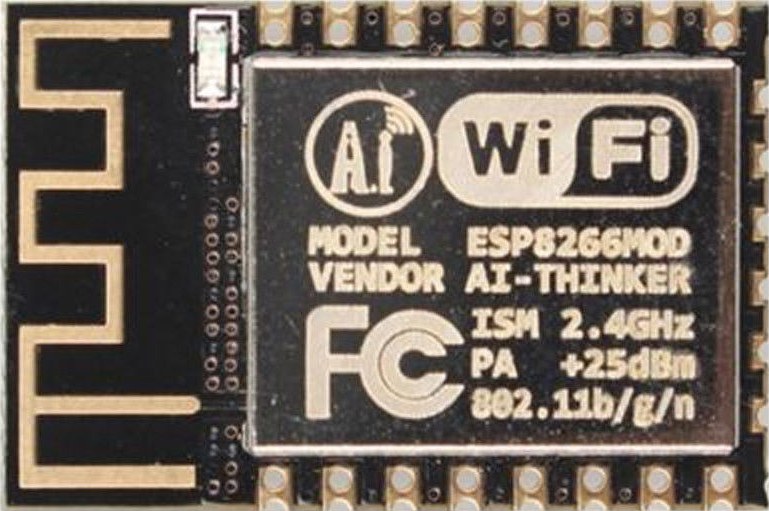
As you see the vendor is the AI-THINKER and the model is ESP8266MOD and most of the times this is what you find in ebay, but you may also find modules with no markings.
MCP6H04
This is an IC with 4x low noise single supply, rail-to-rail output opamps and a voltage range up to 16V, which is more than enough for the purpose. You can find the specs here. This costs around 0.85 EUR for single unit in Arrow or other electronic component distributors. I wouldn’t buy these ICs from ebay.
FDP6030BL
This is a N-channel logic level power MOSFET with a very low Rds(on) (0.018Ω @ 10V). We need a logic level MOSFET because the Vgs needs to be as low as possible. You can find all the specs here. Of course you can use any other MOSFET you like as long as it has the same footprint. That costs approx 1 EUR, but you can use a cheaper one.
MCP4821
This is a low noise 12-bit DAC with an internal VREF of 2.048V, a 2x gain capability and it also has an SPI interface. This thing is a beast. I love it. Easy to use and excellent precision for this kind of projects. This costs ~1.8 EUR. Well, yeeeeeah it’s a bit expensive, I know. We’ll get there soon.
FT232RL
This is a USB to serial IC that supports also the extra hardware signals like DTR and RTS. These are needed actually to simplify the flashing procedure of the esp8266, so you don’t have to use jumpers to put the chip in to programming mode. You can see the trick is used in the schematics, you just need two transistors and two resistors. This costs ~4 EUR… Another expensive component. Not good, not good. There are also other cheaper ones like the CP2102, but they are rare to find because they are very popular in the Chinese vendors that build those cheap USB to UART boards.
PSU
For the power supply we need a couple of stuff. Because the board is USB powered we get the 5V for free from the USB. But we also need 3.3V and 10V. For the first one it’s easy we just need a voltage regulator like the AMS1117-3.3 (or any other variation of the 1117 you can find). For the +10V that are needed to drive the opamps it’s a bit more complicated and for this purpose you need a charge pump IC like the SP6661. This IC can be connected in a way that can double it’s input voltage; therefore if we use the +5V from the USB we can get +10V. The cost of the SP6661 is ~1.5 EUR.
Project source code
The source code is really simple, because I’ve used the arduino libs for the esp8266, therefore I didn’t write much code. Although, for prototyping and also to do quick stuff the arduino libs are nice, I don’t like using them and I prefer to write everything baremetal. Actually, this is how I’ve started the project but at some point I figured out that it needed quite much time for a stupid project. Therefore, I decided to go with the arduino libs.
Originally, I’ve started with the cnlohr’s esp82xx, which although it’s an excellent start template to start with and it has quite a few nice things in there, like a custom small file system and websockets; at the same time it’s a bit tight to it’s default web interface and it’s quite an effort to strip out all the unused stuff and add your own things. Therefore, after already spending some time with this template and bulding on top of it, I’ve decided to go with the arduino libs for the esp8266 because in that case I just had to write literally a few lines of code.
You can find the source code here:
https://github.com/dimtass/esp8266-web-eload
Also the kicad files are in there, so you can edit/order your own board. Read the README.md file for more info how to build the binary and upload the web server files.
Web interface and functionality
Before I’ve build the PCB I’ve tested most of the functionality on a breadboard, just to be sure that the main stuff is working.
Noise, noise, noise
Well, although the esp8266 has an ADC, there are two problems. First it’s maximum input voltage is 1V, which makes it prone to noise from external interference. Second it’s crap. When esp8266 is using it’s WiFi radio to transmit then there’s a lot of noise in the ADC, so much noise that it makes the ADC readings completely unusable even with analog external filters or software low pass or IIR filters. The error can even as much as 4-bit and that’s total crap, especially on low ADC values. Here we can see an image that when the DAC value is 0, then the ADC input is that crap signal.

That’s more than 200mV of noise. But, if I disconnect the RC filter output from the ADC and just probe it, then I get this output.

The noise drops to 78mV, which is still high, but much better than before. Therefore, you see that there’s a lot of noise in the system and especially there’s a lot of noise when the RC filter output is connected on the ADC; which means that the esp8266 creates a lot of noise itself. That’s really bad.
Anyway, the components are already expensive and the price is getting out of the scope for a stupid project, therefore I prefer having this crap ADC input instead of spending more for a low noise SPI 12-bit ADC. In the end of the article I will tell you what is the best option and one of my next stupid projects.
Web interface
That was what the whole project was made for. The web interface… I mean, ok, all the rest of the things could be made much less expensive and with better results in terms of noise, but let’s proceed with this. This is the web interface that is stored in the esp8266 upper 1M flash area.

The upper half of the screen is the ADC read value (converted to volts) and the lower half is the output value of the DAC (also converted to volts). The DAC value is very accurate and I’ve verified with my Fluke 87V in the whole range. I’ve also added a libreoffice calc sheet with the measured values. In real time the ADC value is changing constantly on the web interface, even with the RC filter and also a software low pass filter.
The web interface is using websockets in the background. There are many benefits on using websockets and you can find a lot of references in the internet. The days before websockets, for similar projects, I had to use ajax queries, which are more difficult to handle and also they can’t achieve the high speed comms of the websockets. There are a couple of excellent videos with websockets and esp8266, like this one here.
To control the current that will flow to the load resistors you just need to drag the slider and select the value that you want. You can actually only trust the slider value and just use the ADC reading as an approximate value and just verify that the Vgs is close to the wanted value.
This is the setup on my workbench that I’ve used to build the circuit and run the above tests.
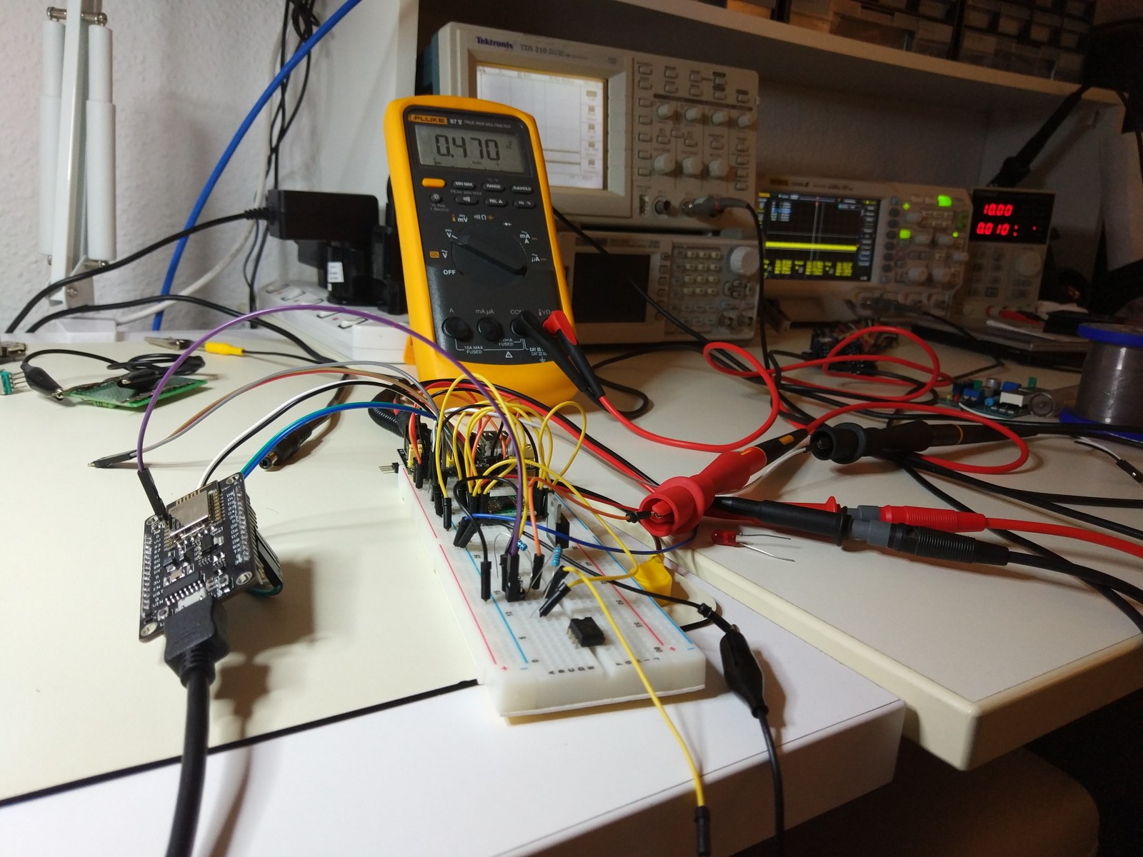
You may see that I’ve solder a pin header pin on the ADC of the esp8266 board. That’s because the Lolin esp8266 board has a voltage divider in the ADC pin in order to protect the input from the 3V3 voltage you may insert as this is the reference voltage for the board.
PCB board
As I’ve mentioned I’ve created a PCB board for that and I’ve ordered it from seeedstudio, which by the time had the cheapest price. So for 5 PCBs, including shipping cost me 30 EUR. This is a 3D image from kicad, but the real one is black. I’ll post it when I get it and assemble it.
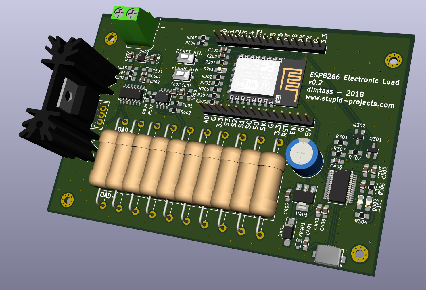
As you can see I’ve exported the same pinout as the Lolin board to make it usabke also for other tasks or tests. The heatsink will be much larger as 9A is quite a lot, but I couldn’t find larger 3D model (I think there’s a scale factor for the 3D model in kicad when you assign the 3D object to the footprint, but anyway).
The maximum current can be set up to 4.095 * 2.2 = ~9A. This is the 2.048 VREF of the DAC, multiplied by 2 with the DAC’s gain and multiplied by 2.2 from the gain of non-inverting opamp amplifier stage. Beware that if you tend to use that high current then you need a very good cooling solution. One way to limit the current in order not to make a mistake is to change the code and use the 1x gain and change also the values in the eload.js javascript file in the web interface. That change will limit the current to 4.5A.
Conclusion
Well, this was a really stupid project. It’s actually a failure in terms of cost and noise. It would be much better to use a microcontroller and replace most of the parts in there. For example instead of using a DAC, the USB-to-serial IC or an external ADC for less noise, you could use a microcontroller that has all those things integrated and also costs much less. For example a nice mcu for this would be the STM32F373CBT6 which has two 16-bit ADCs, two 16-bit DACs, supports USB device connection and other peripherals to use for an SPI display for example. This controller costs only around 5 EUR and it could replace a few parts. Also, you can implement a DFU bootloader to update both firmwares (STM32 and esp8266). Therefore, this might be a future stupid project upgrade. Actually, I’m trying to find an excuse to use the STM32F373CBT6 and build something around it…
Finally the prototype worked for me quite nice and I’ll wait for the board to arrive and test it with my PSU and see how accurate it is. I can’t see any reason why should anyone build this thing, but this is why stupid projects are all about, right?
Have fun!
Comments powered by Disqus.